
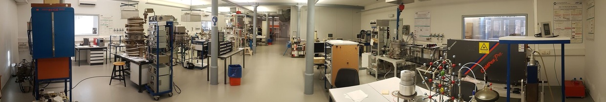
The development and fabrication of superconducting quantum devices - such as cryogenic particle detectors or superconducting quantum interference devices (SQUIDs) - is being driven forward by means of the institute's technology department with integrated clean room. The total area of the dust-reduced technology department is about 300m², of which 60m² is designed as a DIN ISO-5 class clean room. The technologies used in fabrication range from UV photo and electron beam lithography, thin film deposition using magnetron sputtering and thermal and electron beam evaporation to various dry etching methods such as reactive ion etching or ion beam etching.
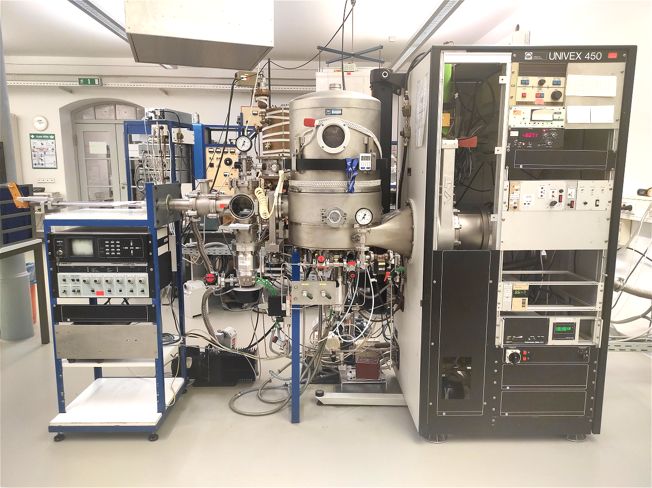
The machinery of the IMS technology department is based on the one hand by commercially acquired systems and on the other hand by self-developed systems optimized for special processes. As a result, the machinery allows for a high degree of flexibility and a wide variety of materials and processes. Currently, the machine park is composed as follows:
- Electron beam lithography system
- Two mask aligners for UV lithography
- One magnetron sputtering system for the production of Nb/Al-AlOx/Nb based Josephson tunnel junctions
- Several deposition systems (magnetron sputtering/thermal evaporation) for superconducting (Nb, NbN, NbTi, NbTiN, Mo, Al, Ti etc.) and normal conducting metals (Au, Cu, AuPd etc.) as well as dielectrics (SiO, SiO2, AlN etc.)
- Fluorine-based RIE system
- Ion beam etching system
- Several wet process tables (with spin coaters, hotplates, convection ovens as well as an ultrasonic and a megasonic bath)
- Equipment for electrochemical anodization
- Equipment for electrodeposition of high purity gold