
Josephson tunnel junctions
A Josephson tunnel junction consists of two superconducting electrodes, the so-called base and top electrode, which are connected by an insulating barrier of a few atomic layers thickness. For an electrical barrier which is sufficiently thin, not only electrons but also Cooper pairs can tunnel through the barrier between both electrodes. As a result of this tunneling process described by the two Josephson equations, highly interesting physical effects occur that are very useful for electronics applications. These include, for example, the Josephson DC effect or the Josephson AC effect, which together with the quantum mechanical tunneling of electrons lead to a current-voltage characteristic that cannot be described by classical methods (see figure 1).
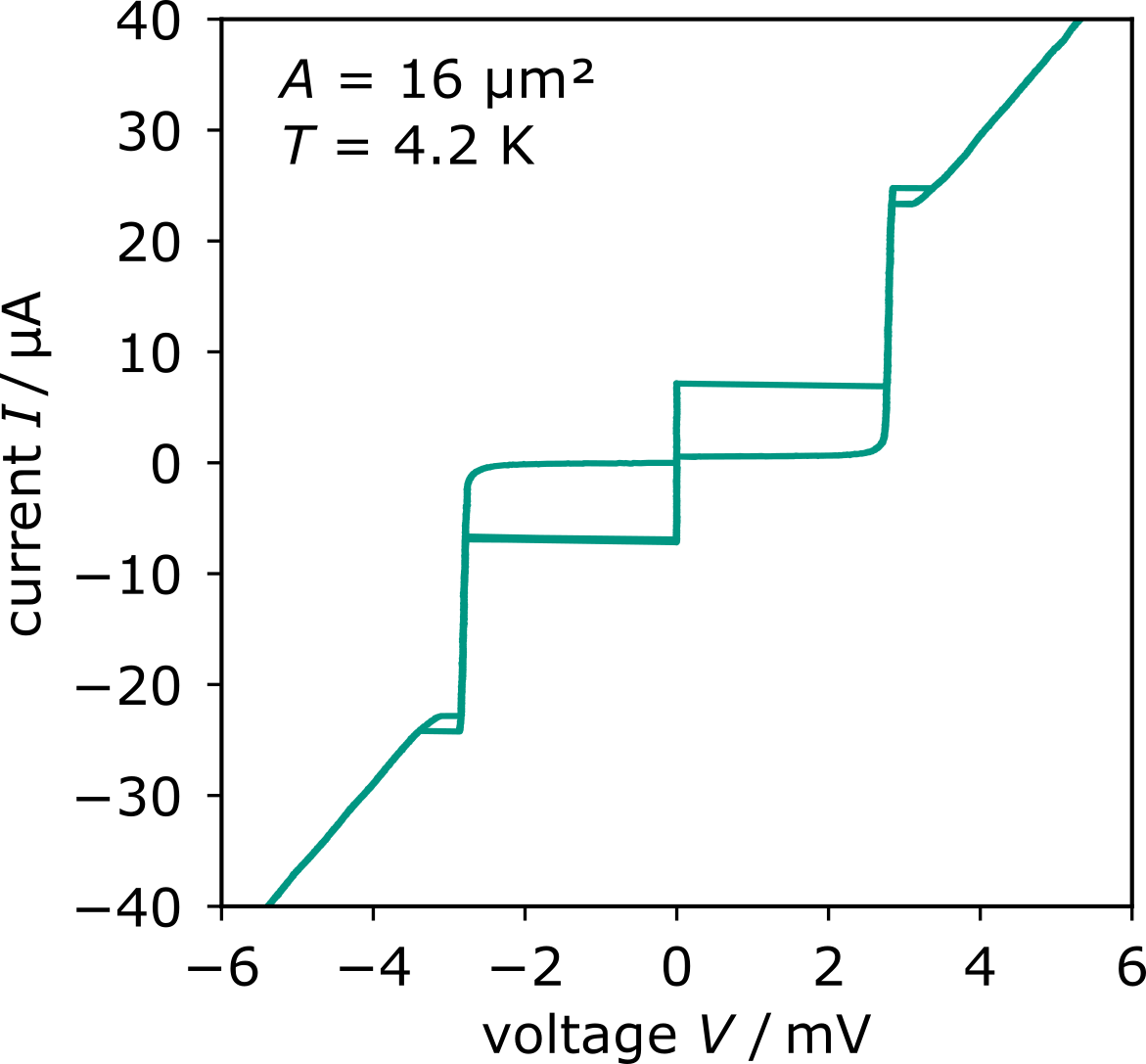
tunnel junction measured at a temperature of T = 4.2 K fabricated at the IMS.
At the Institute of Micro- and Nanoelectronic Systems (IMS), Josephson junctions are used as the basic element for the development of superconducting quantum interference devices (SQUIDs), which can be used to measure changes in magnetic flux. Configured as magnetometers, SQUIDs allow, for example, the measurement of magnetic flux densities down to a few pico- or femtotesla. At the IMS, SQUIDs are primarily used as current sensors.
The Josephson junctions, which serve as the basis for dc and rf SQUIDs developed at the IMS, are fabricated using thin-film technologies available at the institute and basically consist of two superconducting electrodes made of niobium and a tunnel barrier made of aluminum oxide. The fabrication process shown in figure 2 is usually used for this purpose. The actual tunnel junction is structured in the form of a stamp, which is contacted from below and from above by superconducting structures. For the galvanic isolation between the connection to the base and top electrode, the tunnel junction is completely covered with an insulation layer except for a small window in the center of the top electrode. For this reason, Josephson junctions fabricated this way are also called window-type junctions. At the IMS, Josephson junctions with an area of 4 μm × 4 μm are routinely produced in this way. The properties of the Josephson junctions (critical current, normal state resistance, subgap resistance, and gap voltage) can be reliably adjusted on a substrate scale or over multiple fabrication batches, thus enabling the fabrication of complex circuits based on Josephson tunnel junctions.
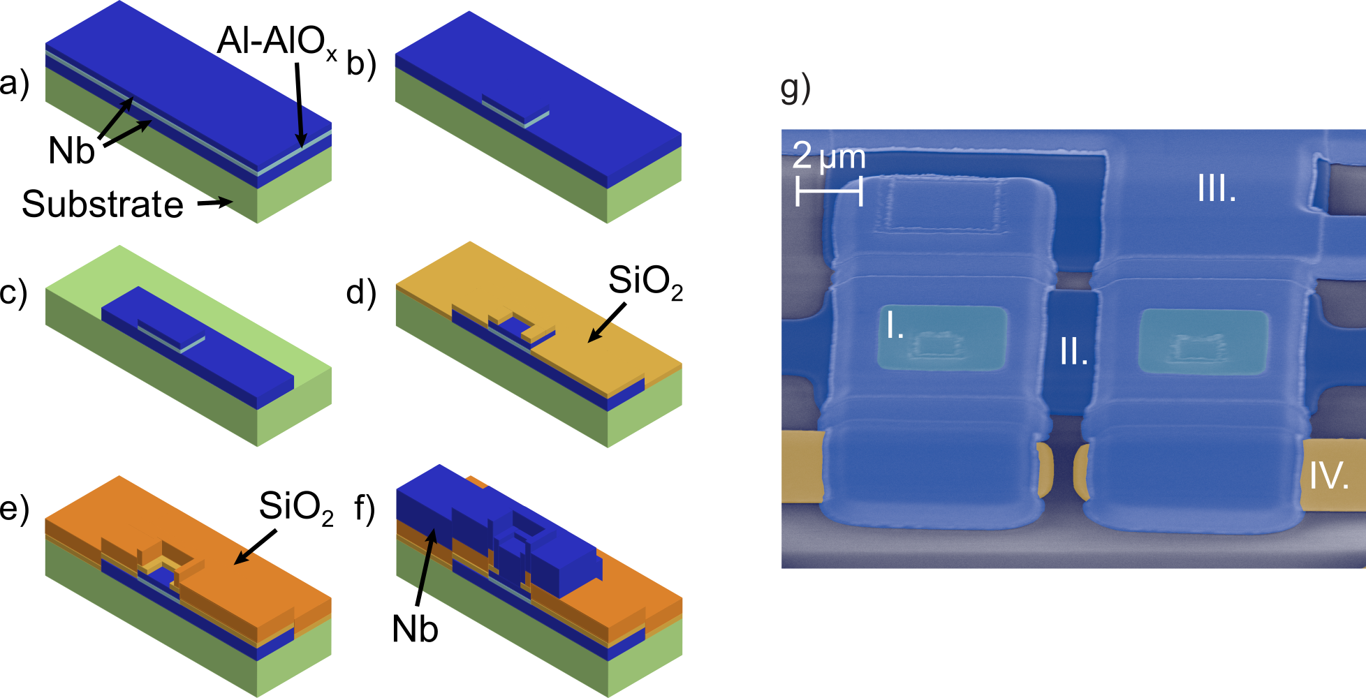
For many applications, however, there is the ambition to minimize the area of the fabricated Josephson junctions because, among other reasons, the capacitance of a Josephson tunnel junction can adversely affect the operation of a SQUID. In this case, alternative fabrication processes must be used since the area of window-type junctions is limited by the size and the alignment accuracy of the isolation window. A possible alternative process was co-developed at the IMS and allows the fabrication of so-called cross-type junctions whose area is limited only by the minimum feature size of the lithography process. With the help of the lithography systems available at the institute, cross-type junctions as small as 1 μm × 1 μm can thus be reliably produced. Josephson junctions with even smaller edge lengths in the range of a few 10nm are possible using electron beam lithography. Currently, intensive work is being done for reaching such small values.
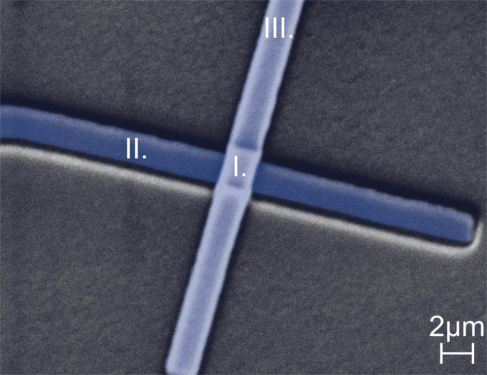
I. Josephson junction. II. Base electrode. III. Contact to the top electrode.
Related publications of the working group:
- Characterization of the reliability and uniformity of an anodization-free fabrication process for high-quality Nb/Al-AlO
Kempf, S.; Ferring, A.; Fleischmann, A.; Gastaldo, L.; Enss, C.
2013.Superconductor science and technology, 26 (6), ref: 065012. - Low-noise current sensor dc SQUIDs with impedance matching for metallic magnetic calorimeters
Bauer, F.
2022, Dissertation, University of Heidelberg. - Development of a metallic magnetic calorimeter with integrated SQUID readout.
Krantz, M.
2020, Dissertation, University of Heidelberg. - Anodization-free fabrication process for high-quality cross-type Josephson tunnel junctions based on a Nb/Al-AlOx/Nb trilayer
Adam, F.; Enss, C.; Kempf, S.
2024, Superconductor science and technology, 37 (8), Art.Nr.: 085013